
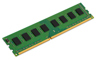
ValueRAM KVR13N9S8/4 memory module 4 GB 1 x 4 GB DDR3 1333 MHz
Non-ECC - CL9 - 1.5V - Unbuffered - DIMM Module
Brand: Kingston
SKU: KVR13N9S8/4
$83.88
Price as listed. Shipping charges calculated at checkout.
In stock

Do you have any question about this product or its specs? Want to know more? Click here to contact our pre-sales consultant and make the right purchase.
 NOTE: The information below is provided for your convenience only; the accuracy of the specifications cannot be guaranteed. However, if necessary, please check with us before purchasing. Data provided by 1 World Sync.
General
Component for
PC/Server
Internal memory
4 GB
Memory layout (modules x size)
1 x 4 GB
Internal memory type
DDR3
Memory clock speed
1333 MHz
Memory form factor
240-pin DIMM
CAS latency
9
Product colour
Green
Kingston Technology ValueRAM KVR13N9S8/4. Component for: PC/Server, Internal memory: 4 GB, Memory layout (modules x size): 1 x 4 GB, Internal memory type: DDR3, Memory clock speed: 1333 MHz, Memory form factor: 240-pin DIMM, CAS latency : 9, Product colour: Green
| Estimate Gross Weight | 0.034 |
|---|
https://www.ec.kingston.com/ecom/hyperx_us/partsinfo.asp?root=&ktcpartno=KVR13N9S8/4
This document describes ValueRAM's 512M x 64-bit (4GB) DDR3-1333 CL9 SDRAM (Synchronous DRAM), 1Rx8 memory module, based on eight 512M x 8-bit DDR3-1333 FBGA compo- nents. The SPD is programmed to JEDEC standard latency DDR3-1333 timing of 9-9-9 at 1.5V. This 240-pin DIMM uses gold contact fingers. The electrical and mechanical specifica- tions are as follows:
- JEDEC standard 1.5V (1.425V ~1.575V) Power Supply
- VDDQ = 1.5V (1.425V ~ 1.575V)
- 667MHz fCK for 1333Mb/sec/pin
- 8 independent internal bank
- Programmable CAS Latency: 9, 8, 7, 6
- Programmable Additive Latency: 0, CL - 2, or CL - 1 clock
- Programmable CAS Write Latency(CWL) = 7 (DDR3-1333)
- 8-bit pre-fetch
- Burst Length: 8 (Interleave without any limit, sequential with starting address ΓÇ£000ΓÇ¥ only), 4 with tCCD = 4 which does not allow seamless read or write [either on the fly using A12 or MRS]
- Bi-directional Differential Data Strobe
- Internal(self) calibration: Internal self calibration through ZQ pin (RZQ : 240 ohm ┬▒ 1%)
- On Die Termination using ODT pin
- Average Refresh Period 7.8us at lower than TCASE 85┬░C, 3.9us at 85┬░C < TCASE < 95┬░C
- Asynchronous Reset
- PCB: Height 0.740ΓÇ¥ (18.75mm) or 1.180ΓÇ¥ (30.00mm)
0.0
0 review(s)
Inside NetworkDistri
From our network to yours.
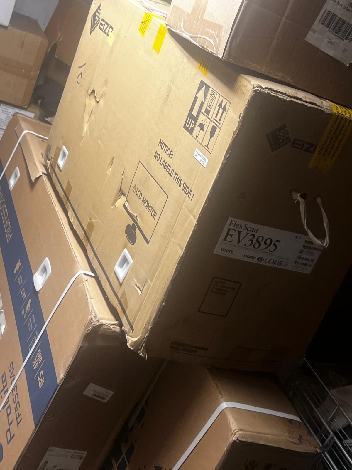
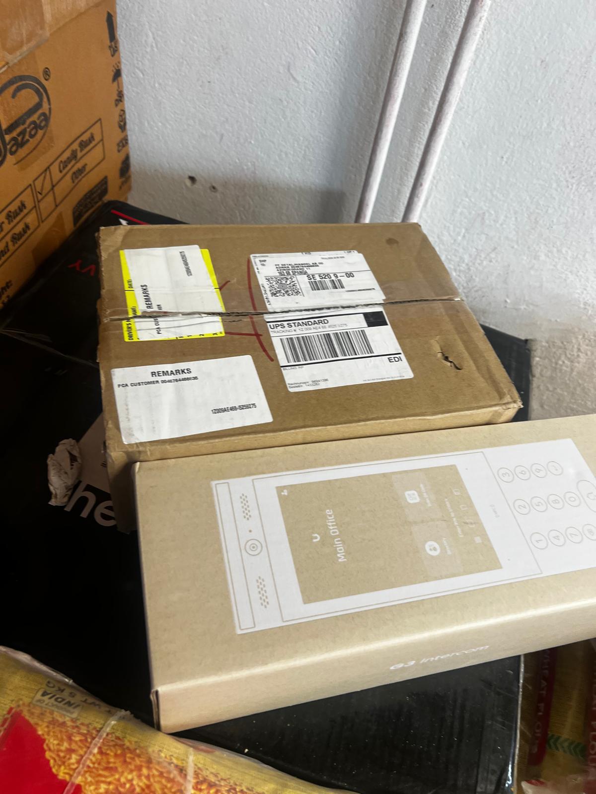
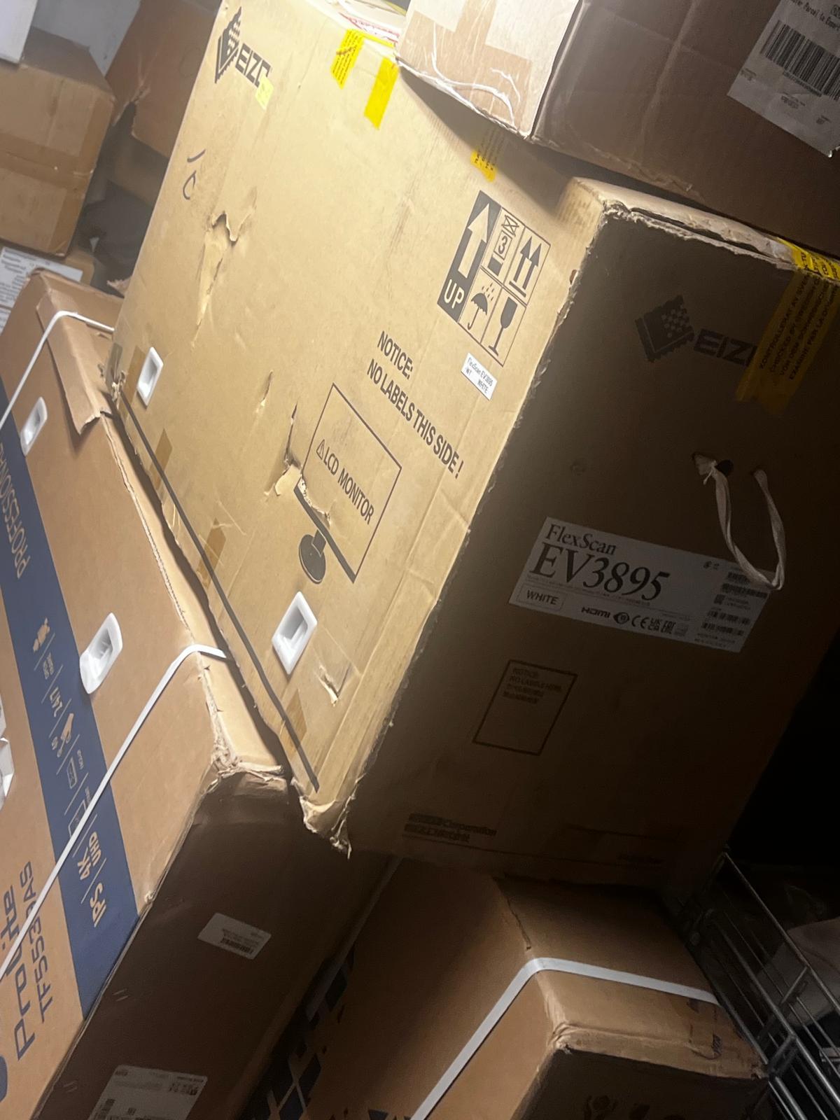
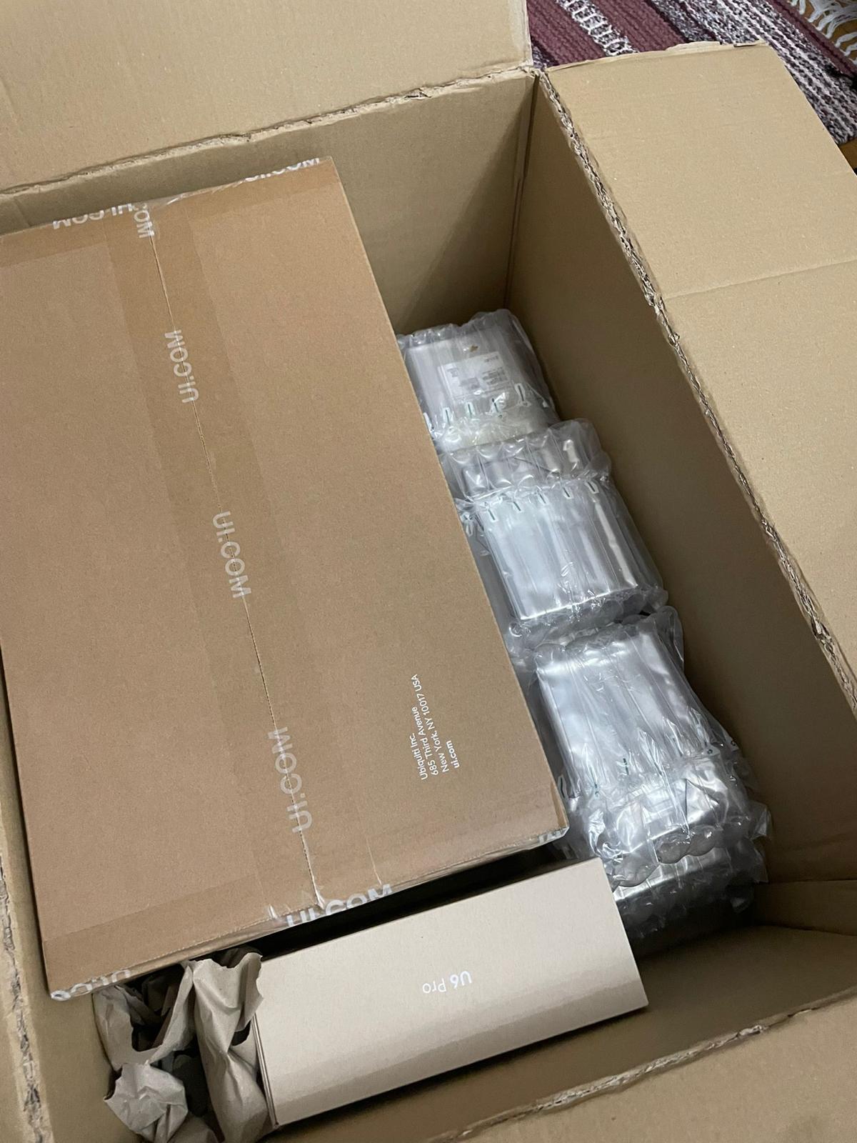
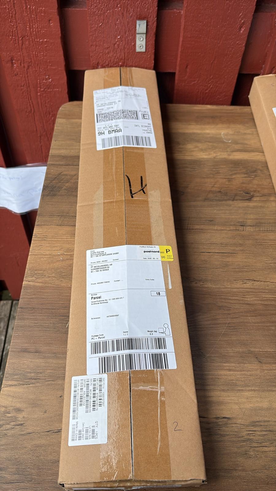
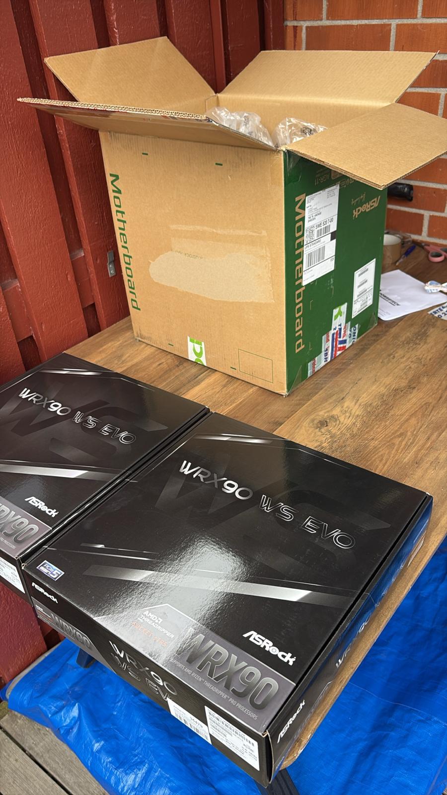
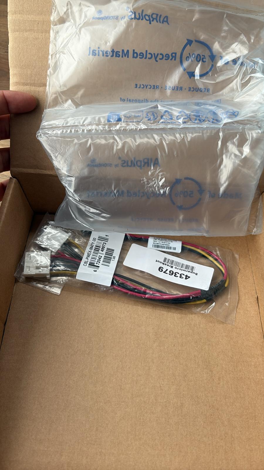
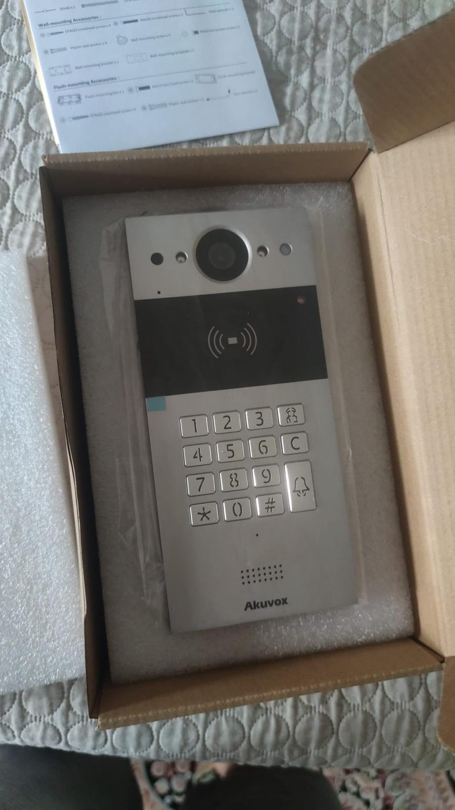
Every day, technology moves through our operation — received, checked, prepared and dispatched to customers. The images below show real equipment handled through our operation, not stock photography.
Real operations
Technology we actually handle
01
Source
Global supply
02
Receive
Goods arrive
03
Prepare
Process & pack
04
Dispatch
On the way